QUANTIN
Epitaxial Quantum materials interfaces for solid-state qubits architectures
Project manager
Simone Assali, CEA
Overview
The aim of the QUANTIN project is to explore new superconducting/semiconducting and superconducting/topological material platforms for quantum devices with improved structural properties and performance.
Keywords: Quantum materials, topological insulators, epitaxy, superconductor, topological semimetal, Tin, Germanium, V-VI materials, Josephson junctions, gatemon qubits
In a nutshell
Engineering materials and devices for solid-state quantum technologies requires a careful control of the interface quality between materials with different physical properties. Any disorder at these interfaces (defects, impurities, and roughness) is a detrimental source of noise and dissipation, and compromises the ability to generate, detect, and manipulate quantum states.
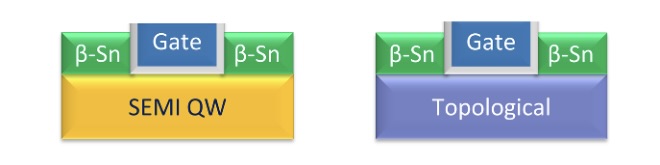
The QUANTIN project will explore novel material platforms for quantum devices with enhanced structural properties and device performance. To this end, QUANTIN will develop high quality interfaces between superconductor/semiconductor and superconductor/topological materials by performing the epitaxial growth in a high purity environment and down to cryogenic temperatures. Tin (Sn) will be used as superconductor due to combination of high critical temperature and resilience to high magnetic fields, thus outperforming widely used Aluminum superconducting contacts in quantum devices. QUANTIN will develop high quality epitaxial junctions between Sn and a variety of III-V, IV, V-VI materials that inherently possess either semiconductor or topological properties. Josephson junctions will be fabricated using these hybrid junctions to unveil the suitability of Sn-based gatemon devices for solid-state qubit manipulation. T
he results of QUANTIN will disrupt quantum hardware technologies and pave the way for novel device architectures with enhanced functionalities that will find applications in superconducting and topological quantum computing.
Challenges
- Realize a β-Sn superconducting layer with improved structural quality by performing epitaxial growth at cryogenic temperature on Ge 2DHG, InAs 2DEG and BiSb quantum materials, and to enrich the knowledge on the superconducting properties of β-Sn.
- Fabricate superconducting/semiconducting (β-Sn/Ge 2DHG, β-Sn/InAs 2DEG) and superconducting/topological (β-Sn/BiSb) JoFETs and demonstrate their suitability for solid-state quantum technologies.
Tasks
- WP1: β-Sn/Ge 2DHG SC/SEMI junctions
- WP2: β-Sn/III-V 2DEG SC/SEMI junctions
- WP3: β-Sn/Bi1-xSbx SC/TOP junctions
- WP4: JoFETs fabrication and quantum transport measurements
Consortium
- CEA DEPHYS
- Direction de la recherche fondamentale (CEA DRF)
- Institut de recherche interdisciplinaire de Grenoble (CEA Irig)
- Institut Néel (CNRS)
- Laboratoire d’analyse et d’architecture des systèmes (LAAS, CNRS)
- Laboratoire de Physique des Solides (LPS, CNRS / Université Paris-Saclay)
- Laboratoire PHotonique ELectronique et Ingénierie QuantiqueS (PHELIQS, CEA / Grenoble-INP / Université Grenoble Alpes)