e-DIAMANT
Technology network for scientific and industrial applications of diamond sensors
Project manager
Jean-François Roch, ENS Paris-Saclay
Overview
EquipEx+
e-DIAMANT federates the knowledge and expertise of 11 partners to create diamond samples optimized for quantum applications. In particular, the project exploits structural defects in diamond as quantum sensors based on artificial atoms.
Keywords: diamond NV centers, quantum sensors, ion implantation, optical microcavities, nano-magnetism, paleo-magnetism, high-pressure physics
In a nutshell
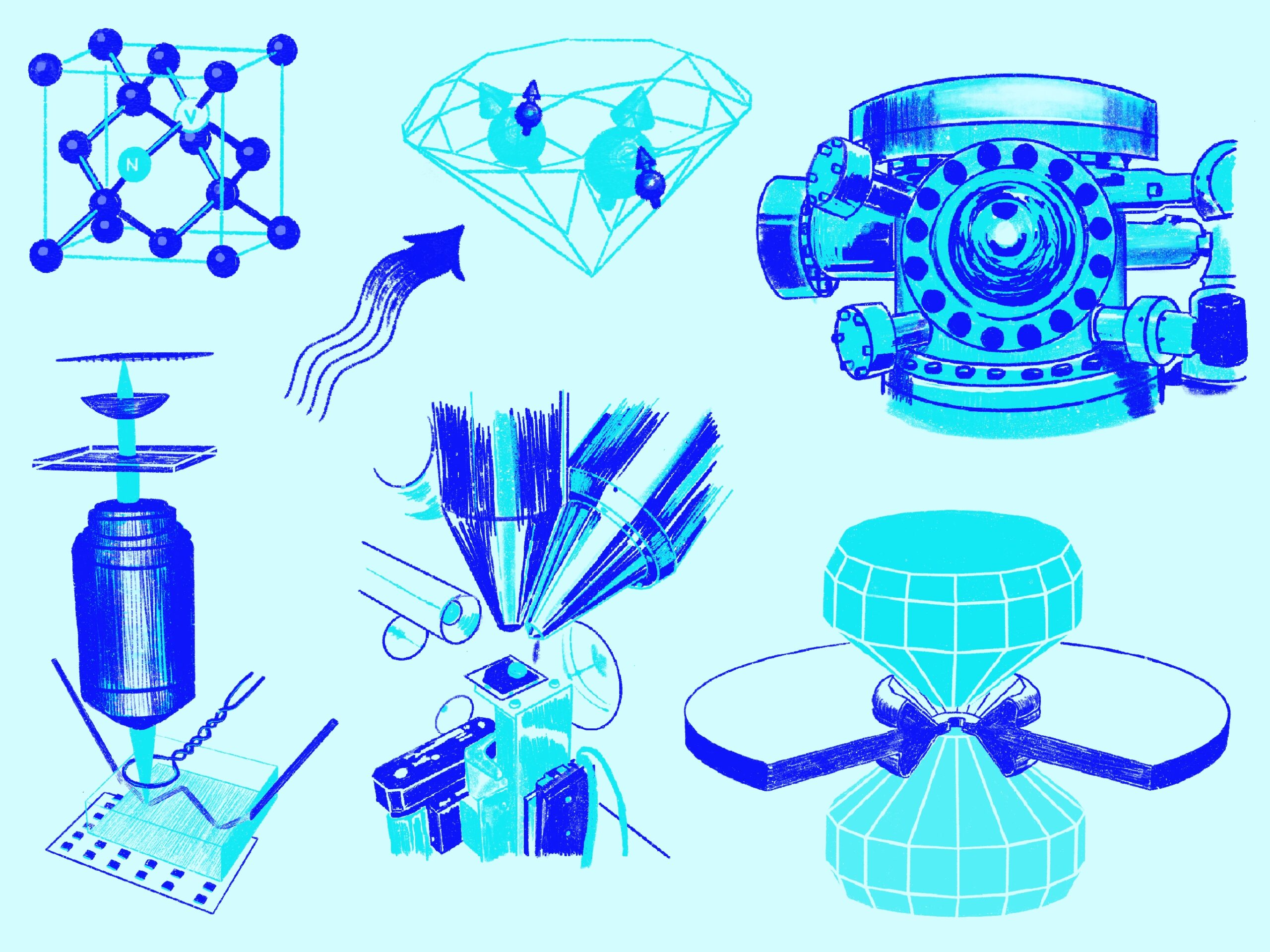
The NV center in diamond consists of a substituted nitrogen atom associated with a vacancy. Among the several hundred or more existing defects in diamond, the NV center possesses unique properties. It offers the possibility of coherently manipulating electron spins in the solid state at room temperature, with direct optical readout. As the coupling of the spin to an external magnetic field modifies its state, the NV center behaves like an atom, with a magnetic field sensitivity of a few nT and spatial resolution on the nanometer scale.
The study of this system and the development of the first devices have already opened up new fields of investigation in a wide variety of fields. Since magnetic fields exist almost everywhere, the use of the NV center as a magnetic sensor can provide solutions to societal and economic needs for which no viable approach yet exists. Examples include:
- The ability to characterize new condensed matter structures such as those developed for spintronics.
- Elucidate chemical structures by extracting nuclear magnetic resonance (NMR) from single molecular entities. This will open up new possibilities for drug development and disease diagnosis.
- Demonstrate superconductivity phenomena at room temperature, by monitoring the new states of matter created by applying pressures of up to 600 GPa.
- Carry out magnetic measurements to contribute to progress in Earth and planetary sciences.
Beyond these fields of investigation, there are probably many others yet to be discovered and invented. The e-DIAMANT project will use the complementary know-how and expertise of the partners to create a set of tools for obtaining a diamond material with a controlled level of defects, optimized design and dimensions.
Challenges
- Make France a world-leading supplier of diamonds for scientific applications, useful for both classical and quantum sensors. In particular, the samples studied, manufactured and characterized by this new technology platform will enable the development of quantum sensors with new detection functionalities.
Tasks
- Node 1: Growth and cutting of diamond
- Node 2: Post-processing for quantum defect enhancement of diamond
- Node 3: Precise spatial positioning of diamond defects
- Node 4: Nano-structuring of diamond
- Node 5: Control of position and quality of diamond defects
- Node 6: Applications to magnetic measurements and other new functionalities
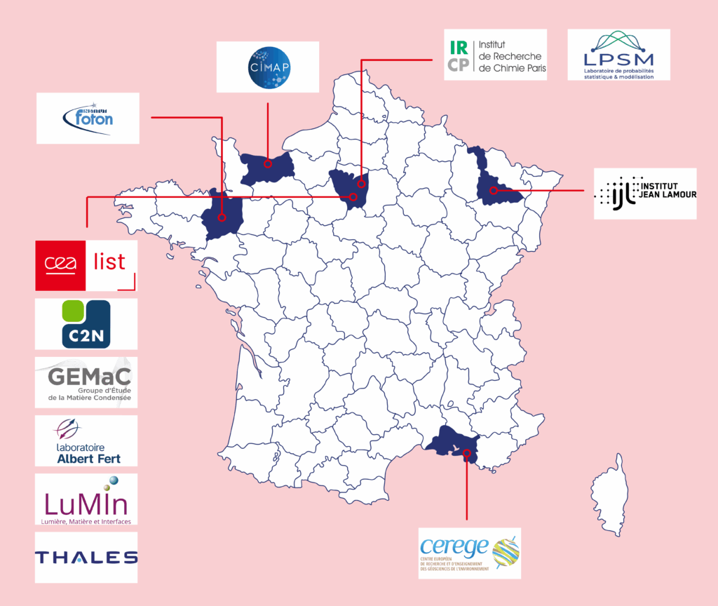
Consortium
- CEA-LIST (Institut Carnot / Université Paris-Saclay / Université Grenoble Alpes)
- Centre de Nanosciences et de Nanotechnologies (C2N, CNRS / Université Paris-Saclay)
- Centre de Recherche et d’Enseignement des Géosciences de l’Environnement (CEREGE, Aix-Marseille Université / CNRS / INRAE / IRD)
- Centre de recherche sur les ions, les matériaux et la photonique (CIMAP, CEA / CNRS / ENISCAEN / Université Caen Normandie)
- Groupe d’études de la matière condensée (GEMaC, CNRS / Université Versailles Saint-Quentin-en-Yvelines)
- Institut de Recherche de Chimie Paris (IRCP, Chimie ParisTech-PSL / CNRS)
- Institut Fonctions Optiques pour les Technologies de l’information (Institut FOTON, CNRS / INSA Rennes / Université de Rennes)
- Institut Jean Lamour (IJL, CNRS / Université de Lorraine)
- Laboratoire Albert Fert (LAF, CNRS/ Thales)
- Laboratoire de Probabilités, Statistique et Modélisation (LPSM, CNRS / Sorbonne Université / Université Paris Cité)
- Laboratoire Lumière-Matière aux Interfaces (LUMIN, CNRS / ENS Paris-Saclay / Université Paris-Saclay)